
Most Custom AI Silicon Will Be Stranded Within Three Years
The physics of chip fabrication and the pace of algorithmic change are on a collision course. Billions of dollars are on the wrong side of it.
Most people building AI infrastructure are thinking about the stack from the software layer down. Which model, which framework, which cloud provider. The chip is treated as a commodity input. The assumption is that once you pick one, the physics underneath will keep cooperating
I used to think that too.
Before starting Cosmic, I worked on quantum sensing and navigation systems, where hardware operates at the absolute edge of what physics permits. That experience made me skeptical of abstractions. When someone tells me a system performs a certain way, my first question is: what physical phenomenon is doing that work, and what happens when the physics stops cooperating?
Right now, billions of dollars are flowing into custom AI chips. And today, I work with infrastructure teams across national laboratories and large-scale compute environments. The pattern is consistent: hardware that was right at procurement is already drifting from the workloads running on it. I think a very large amount of the custom AI silicon being taped out today will be functionally stranded within 36 months. Not because the chips are bad, but because the physics and the algorithms are moving in directions that will make the hardware assumptions underneath them wrong. This piece explains why.
The industry has massively underinvested in the operational layer between silicon and software. The stranding problem described in this piece is going to make that gap a lot more expensive.
The Transistor Is Fighting Physics
A transistor is a gate. Apply voltage, current flows. Remove it, current stops. Stack a billion on a chip the size of a thumbnail and you have a computer. Making transistors smaller made them faster and cheaper for decades, because electrons at those scales behaved like classical particles and the engineering intuitions held.
That era is over. Modern process nodes like “2nm” and “3nm” are marketing labels, not measurements. Actual channel widths sit between five and fifteen nanometers, roughly twenty to fifty silicon atoms across. At those dimensions, electrons behave like waves and can tunnel through energy barriers they shouldn’t classically cross. The transistor never fully turns off. Across billions of transistors, that leakage becomes a real fraction of total power draw even at idle.
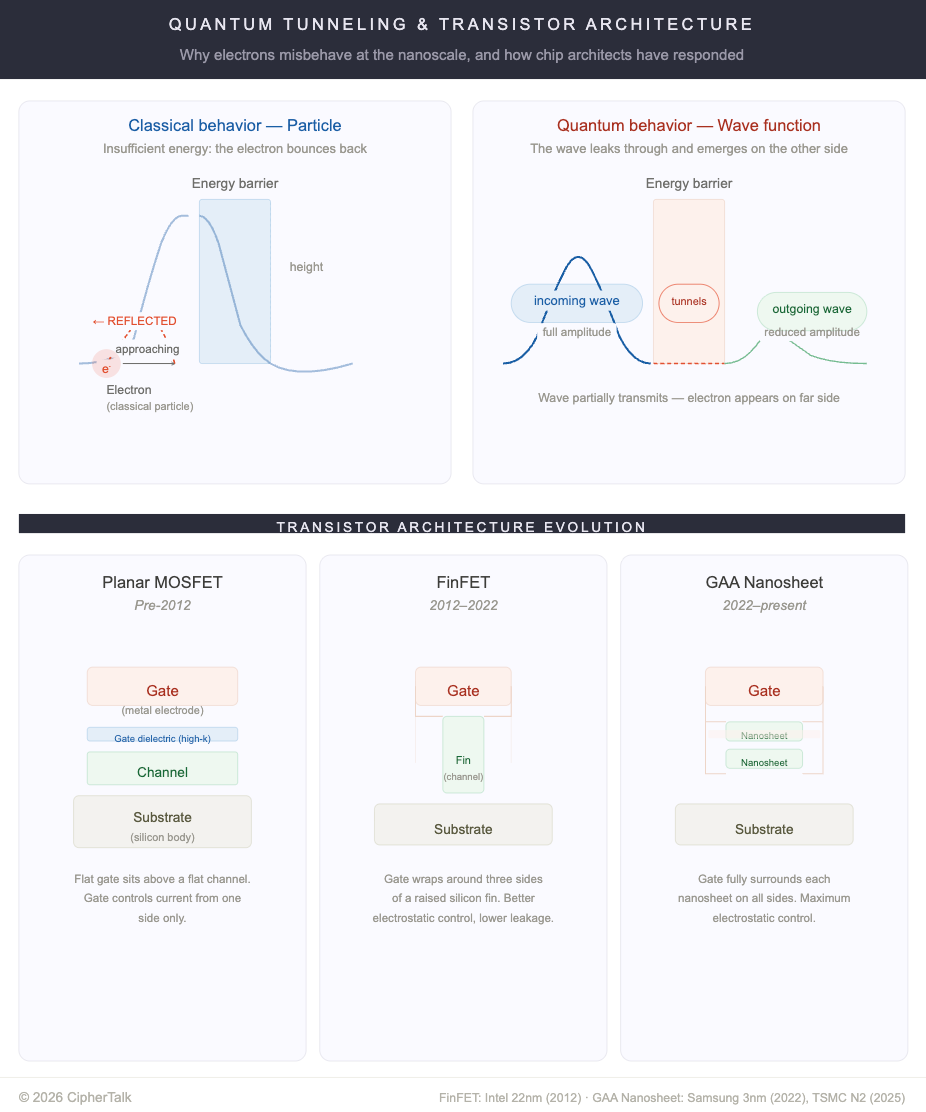
A 2024 paper in Nature Nanotechnology from Queen Mary University and Oxford showed that direct source-to-drain tunneling degrades switching behavior and caps operating frequency due to rising static power dissipation. The same team built a transistor whose channel is a single zinc porphyrin molecule, using destructive quantum interference (two electron pathways through the molecule cancel each other out) to suppress leakage. This is quantum mechanics recruited as the switching mechanism rather than fought against. It’s a laboratory result, not manufacturable, but it demonstrates a path that works with physics.
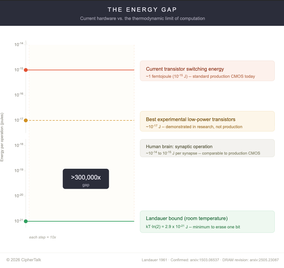
There is also a thermodynamic constraint. In 1961, Rolf Landauer showed that erasing one bit of information must release heat, a consequence of the second law of thermodynamics. This was experimentally confirmed in 2012, and the minimum energy (called the Landauer bound) sits at roughly 2.9 × 10⁻²¹ joules per bit at room temperature. Current transistors dissipate about one femtojoule per switch, a gap of over 300,000x. But a 2025 paper measuring erasure energy in real silicon DRAM (dynamic random-access memory, the working memory inside every computer) at single-electron resolution found the Landauer limit wasn’t reached even under effectively infinite-time operation, because DRAM cells can’t prepare their initial charge state in thermal equilibrium. Since that circuit topology appears broadly across electronic design, the theoretical floor for energy efficiency in real circuits may be significantly higher than the Landauer bound suggests, which means projections that extrapolate current improvement curves toward the Landauer floor are probably wrong.
These physical constraints mean each generation of silicon is more expensive to fabricate, more thermally fragile, and harder to repurpose when the workload it was designed for changes. That last point is where the money is.
Why Custom AI Silicon Gets Stranded
An ASIC (application-specific integrated circuit) strips out general-purpose overhead and builds exactly the circuits a particular workload needs. For dense matrix multiplication (the core math operation in AI training and inference), the efficiency gains over a GPU (graphics processing unit, the general-purpose chips most AI runs on today) can be an order of magnitude per watt. That’s real. Groq, Cerebras, and dozens of stealth startups have raised billions on this premise. Internal efforts at the hyperscalers are following the same logic.
The problem is the clock. ASICs take two to three years from architecture freeze to first silicon. Model architectures are now shifting faster than that.
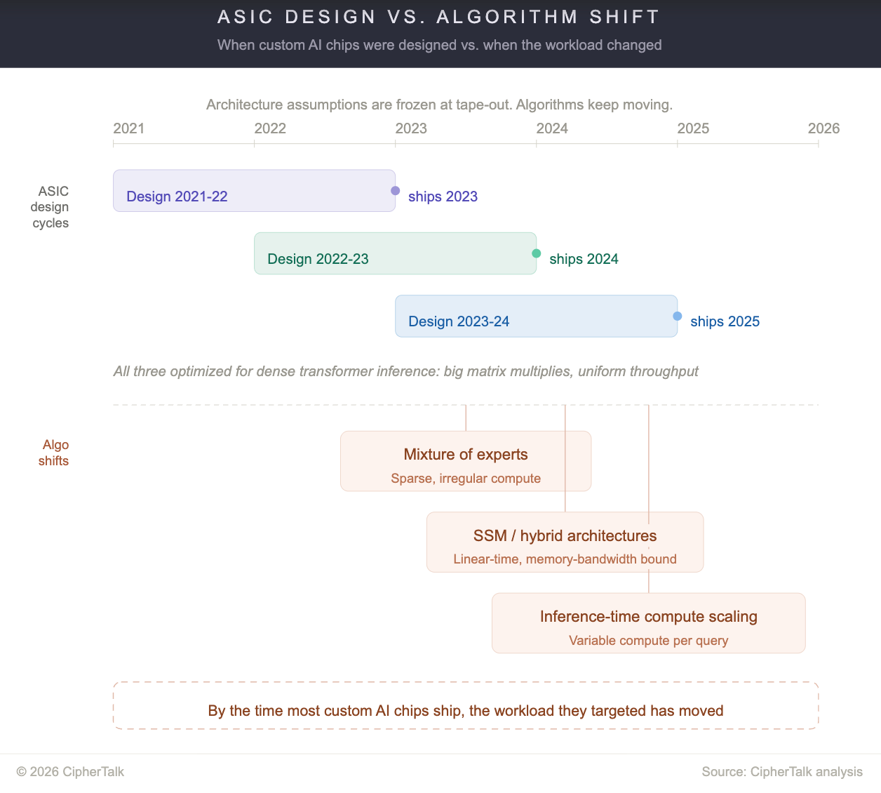
When most of today’s AI ASICs were designed, the dominant paradigm was dense transformer inference: big matrix multiplies, regular memory access patterns, predictable compute-to-memory ratios. That’s no longer the only game. Mixture-of-experts models (architectures where only a small subset of the network activates for each input) like DeepSeek-V3 activate only a fraction of their parameters per token, which means compute is sparse and irregular, not dense and uniform. State space models (a class of sequence models that process inputs through a compressed internal state rather than attending to every prior token) and hybrid architectures are replacing quadratic attention with linear-time alternatives that have fundamentally different hardware profiles. Inference-time compute scaling, where models spend variable amounts of compute per query depending on difficulty, breaks the fixed-throughput assumptions ASICs are designed around.
A chip optimized for dense matrix multiply doesn’t help much when the workload is sparse routing across 256 experts, or when the bottleneck is memory bandwidth for the model’s compressed internal state, or when inference compute varies 10x between queries. The silicon is still good. The assumptions baked into it are wrong.
Consider Groq's LPU. The architecture is built around deterministic execution: every operation is statically scheduled by the compiler before runtime, all model weights live in on-chip SRAM with no external memory, and the hardware assumes a fixed, predictable dataflow through sequential transformer layers. For dense, single-model inference on a standard transformer, this design delivers extraordinary latency. But deterministic static scheduling is the opposite of what you want when inference-time compute varies per query, or when MoE routing sends different tokens to different experts based on input content that can't be known at compile time. The architecture's greatest strength, total elimination of runtime variability, becomes its limitation when the workload is variable. In December, NVIDIA agreed to pay $20 billion to license Groq's technology and hire its founder and senior leadership, in what analysts described as a de facto acquisition structured to avoid antitrust scrutiny. You can read that two ways: NVIDIA saw durable value in the inference IP, or the market signaled that the standalone path for a single-workload inference ASIC was narrowing fast enough that consolidation was the better exit.
Power makes this worse. At sub-10nm nodes, a phenomenon called “dark silicon” means that more than half of a chip’s transistors must be powered off at any moment to stay within thermal limits. The industry response has been to pack specialized accelerators that power on only when their workload arrives. But when the workload evolves, those accelerators become expensive dead area.
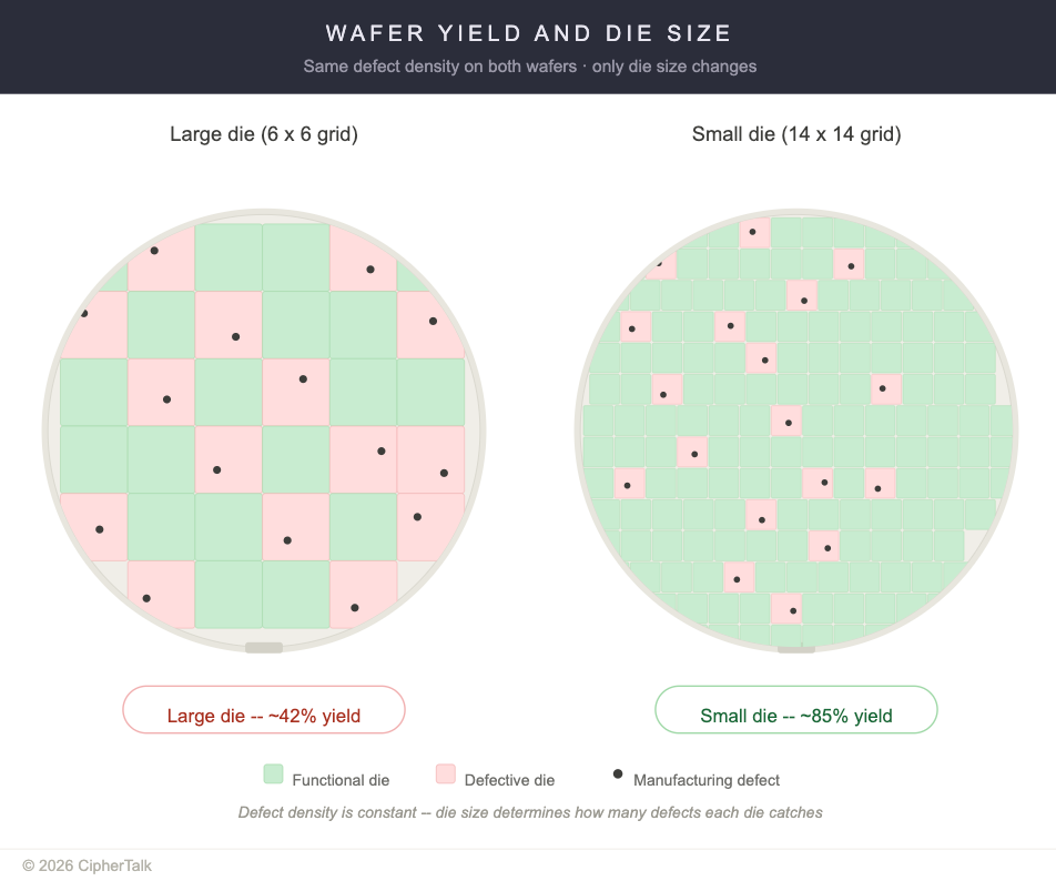
And yield is the financial multiplier. Defect density is roughly constant per unit area of silicon, so larger dies catch more defects per die. A wafer of large dies might yield 42%; the same wafer cut into smaller dies might yield 85%. Advanced-node AI chips tend to be large. The broken ones cost the same to manufacture as the working ones.
Quantum Error Correction: Real Science, Wrong Timeline
A qubit (quantum bit, the basic unit of quantum information) can exist in a blend of 0 and 1, but that blend is extraordinarily fragile. Error correction spreads each logical qubit across many physical qubits so damage can be detected and repaired, but the math only works if physical error rates stay below a critical threshold.
In 2024, Google’s Willow processor (a superconducting chip) and a Microsoft-Quantinuum trapped-ion system (which uses individual charged atoms held in place by electromagnetic fields) both demonstrated below-threshold error correction in hardware. In November 2025, a Harvard-led team published in Nature the first system combining all core components of fault-tolerant quantum computing in a single 448-atom processor.
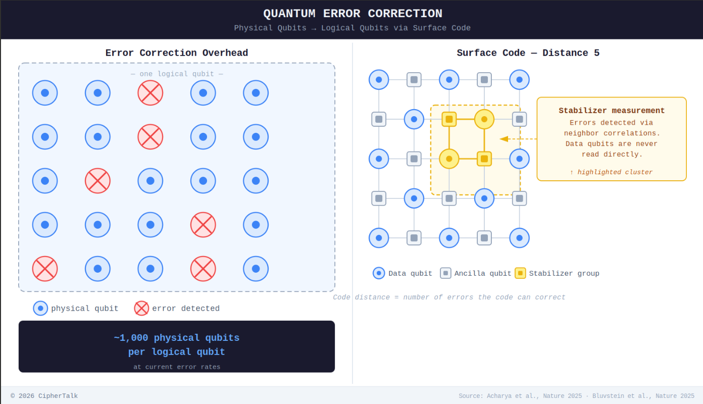
These are genuine scientific milestones. But even Willow’s best logical error rate (around 0.14% per cycle for its distance-7 code) is still orders of magnitude above the ~10⁻⁶ levels needed for useful algorithms. The gap between “below threshold” and “commercially useful” is enormous, and the press coverage collapses it in ways that are moving real capital toward quantum and away from the near-term hardware operations problems that are actually solvable right now. Practical quantum computation remains uncertain by years, probably a decade or more. For anyone making infrastructure investment decisions on a five-year horizon, quantum is not a factor.
The physical world doesn’t hold still for your procurement cycle.
Every section above circles the same point. I see this in practice constantly. A chip that passed qualification at 25°C behaves differently at 68°C in a dense enclosure six months into sustained inference. A fleet of nominally identical accelerators drifts in performance, thermal behavior, and failure modes until jobs that ran on one node fail silently on another. Tooling built for one chip generation breaks when the next one ships. None of this is surprising if you think about hardware as physics rather than abstraction, but most infrastructure teams don’t have time for that framing. They’re firefighting.
That’s the space we at Cosmic operate in: making hardware that’s already in the ground actually work, across vendors and chip generations, even as the workloads running on it move out from under it. But the broader point isn’t about us. It’s that the industry has massively underinvested in the operational layer between silicon and software. The stranding problem described in this piece is going to make that gap a lot more expensive.
Movellus develops intelligent clock networks for chips: https://finance.yahoo.com/news/movellus-partners-synopsys-deliver-power-150000615.html Intel seems to have a similar DVFS.
I really enjoyed reading this, I'm always learning something new when reading your work! This aligns with what I've thought despite me not being a tech person by any means. It's *very* interesting to me that banks + PE houses are underwriting billlions in chip-backed loans (or collateralised chip obligations [CCOs] as I like to call them) based on rapidly depreciating tech. I'm publishing a piece that explores the math of CCOs in a few days too.